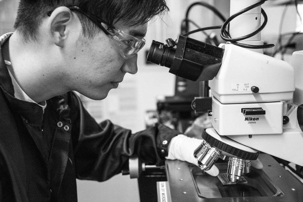
Many of our microfabrication steps (electroplating, polymer casting….) and device characterization are performed in our research labs, which are located in the Krishna P. Singh for Nanotechnology, the Laboratory for Research on the Structure of Matter (LRSM) building, and Skirkanich Hall, at the corner of 33rd and Walnut Street, Philadelphia, Pennsylvania.
Below is a list of our major equipment per research lab. The manuals of some listed equipment can be found here.
Lab – 1 (Singh 205)
- Spinner
- Spray Coating
- Electrospinning
- Electrophoresis
- UV-LED Photolithography
- Polymer Drawing Station
- Flow Hood
- Vacuum Chamber
- Thermforming Station
- Microscope
- Probe Station
- Cyclic Voltammetry
- High-field Electromagnets
- RF Amplifier
- CO2 Laser Cutter
- Spectrum Analyzer
- 3D printer
- Vacuum Oven
- Ovens
- Plating Stations
- Robotic Plating Station
- Glovebox for plating
- Table-top Electromagnet
- Flow Hoods
- Vacuum Chamber
- Optical Microscope
- Thermal Evaporator
- Network Analyzer
- LCR Meter
- Ultrasonic Cleaner
- Incubator
- Mechanical Testing System
- Oscilloscope
- Isotemp Incubator
- Scanning Hall Probe System
- Gaussmeter
- Laser Micrometer
- Dynamic Signal Analyzer
- Spectrum Analyzer
- Flow Hood
- Polymer Synthesis Station
- Diamond Saw
Lab 4 (SKIR 230)
- Optical Microscopes
- Box Furnace
- Annealing Furnace
- Oxidation Furnace
- Residual Gas Analyzer (RGA)
- Lamination Press
- CNC Milling Machine
- High-Precision Scales
- Impedance/Gain-Phase Analyzer
- LCZ Meter
- Magnetic Core Measurement
- Wireless Sensor Read-out Strip
The Laser Micromachining Center is managed by the Quattrone Nanofabrication Center and is located in the Singh Center for Nanotechnology. Two laser systems comprising of three lasers – 193-nm excimer, 532-nm green fiber, and 1070-nm IR fiber – are currently available (see descriptions below). Supporting equipment for sample preparation and analysis are also available. The center is open to authorized internal and external users. We offer basic and advanced training sessions and provide technical support. For more information, please contact us.
Projects previously machined on lasers within MSMA include microneedles, interdigitated and planar metal designs, sintered multi-layer alumina devices, silicon device trimming, and sintered powder permanent magnets. The systems can be used for a wide variety of micromachining applications including micro-drilling, thin film removal, dicing, annealing, laser lift-off (LLO), photovoltaics/solar cells, plastic marking, materials processing, texturing, Si ablation, spot/seam/micro- welding, metal drilling, cutting, batteries, medical devices, and computer components, just to name a few.
The Quattrone Nanofabrication Facility supports nanoelectronics, nanomaterials development and integration, soft matter, microfluidics and MEMS/NEMS.
QNF resides in the Krishna P. Singh Center for Nanotechnology. By providing core nanofabrication capabilities, our mission is to enable research and development in a number of areas. As embodied in the Penn Compact, QNF focuses on increased access, as well as integrating knowledge by engaging the Greater Philadelphia Region and far beyond. Our core endeavors are to support teaching, research, service and commercialization at the micro- and nanoscale.
QNF staff operates a 10,000sq.ft. cleanroom with leading-edge equipment capable of electron-beam and optical lithography, physical and chemical vapor deposition, dry and wet processing, metrology, and device characterization. In addition, a complimentary facility for soft materials and laser micromachining is maintained by QNF for diverse materials processing, microfluidics and lab-on-chip activities. For device packaging and hybridization, there is a suite of backend equipment available for wirebonding, wafer bonding, electrical testing and wafer dicing.
The Singh Center for Nanotechnology, where the MSMA Group is headquatered, is centered around four major research facilities, all featuring state-of-the-art equipment for nanoscale characterization, measurement, and fabrication: the Quattrone Nanofabrication Facility, the Nanoscale Characterization Facility, the Scanning and Local Probe Facility, and the Material Property Measurement Facility.
The following connected sections comprise the major components of the building:
- A 10,000 square-foot next-generation Cleanroom Facility for micro/nanofabrication, including tooling for nanoscale and soft materials integration and a novel nano/bio bay serves as the home of the Quattrone Nanofabrication Facility.
- A 10,000 square-foot advanced underground facility designed for temperature stability and excellent isolation from vibrational, acoustic, and electromagnetic noise serves as home of both the Nanoscale Characterization Facility and the NBIC Scanning and Local Probe Facility.
- A Property Measurement Facility provides state-of-the-art measurement capabilities in magnetometry, optics, electrical and thermal transport.
- 18,000 net square feet of space for other shared facilities and general laboratories housed in an adjoining three story structure; a glass-enclosed galleria with views into the cleanroom; conference rooms; and a forum for meetings.
The building houses a large suite of high-performance equipment for nanotechnology research, including electron and scanning probe microscopy, cleanroom tools, electron beam lithography, and several materials synthesis and characterization instruments.
The multi-user facilities are vital to the research and educational programs at Penn and are leveraged by partner institutions and local industry within the Mid-Atlantic region. Unifying these central resources fosters the exchange of scientific ideas and the development of nanoscale science and technology, brings together crosscutting capabilities and the staffing to support these tools, and provides the modern infrastructure necessary to establish a regional center for nanotechnology.
