
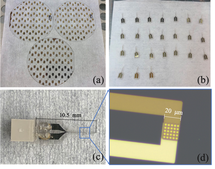
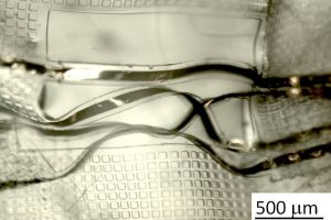
Rapid, point-of-care diagnostic measurement of cytokines in vivo would advance patient care. A desirable approach to this measurement would be a transdermal or transvascular sensor fabricated in the shape of a needle, in which the sensing portion is formed on the needle tip and extends into the body medium of interest upon insertion. When contemplating the sensing approach for such a sensor, it is important to maintain a high degree of specificity to the protein of interest. Electronic-based sensing is a promising approach for femtomolar level specific detection of proteins due to its low cost, ease of miniaturization, and label-free operation. We’re developing a wafer-level microfabricated, needle-shaped impedance sensor for rapid, label-free detection of cytokines and other biomarkers. The sensor, consisting of a 20 μm x 20 μm micro-well array comprising 25 individual 2 μm-diameter wells embedded in a sensing tip, is lithographically configured on a laser micromachined fused silica needle. Label-free specific detection is achieved via functionalizing the microwells with antibody and monitoring the impedance change across the sensor electrodes due to the binding of target protein to the antibody.
Conference paper:
- N. Song, P. Xie, H. Oh, W. Shen, M. Javanmard and M. G. Allen, ” Wafer-Level Micromachining of Insertable, Label-free Cytokine Sensing Platforms”, BMES Annual Meeting, Philadelphia, USA, Oct. 2019.
- Song, P. Xie, M. Javanmard and M. G. Allen, “Microwell-array on a Flexible needle: a Transcutaneous Insertable Impedance Sensor for Label-Free Cytokine Detection”, MEMS 2018, Belfast, UK, Jan. 2018. (PDF).
Human brains are bottom-up synthesized machines that utilize highly complex networks of simple computational units i.e. neurons for cognitive processing. Artificial neural networks, which borrow aspects of this network topology, have already successfully demonstrated human-level classification performances in image and speech recognition tasks. However, implementing these networks on existing computer architectures with markedly different topologies leads to increased power consumption and sub-optimal operating speed. Recent efforts have evolved specialized transistor-based “neuromorphic” circuits that sacrifice the scalability of bottom-up fabrication technologies for the determinism of their top-down counterparts. In contrast, we are designing all-passive, transistor-free circuits that are amenable to the inherently stochastic but scalable bottom-up fabrication approaches. We are investigating the performance of these circuits on benchmark datasets and we are exploring simple fabrication techniques to realize them. The results of our research, we believe, will establish new methods for designing systems that embody intelligence at the physical level.
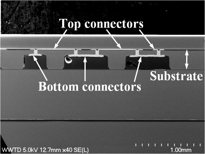
Buried Interconnects
3-D Silicon Integration
Project Overview
In-Silicon Copper Circuitry
Publications
- C.-H. Ji, F. Herrault, P. Hopper, P. Smeys, P. Johnson, M.G. Allen, “Electroplated Metal Buried Interconnect and Through-Wafer Metal-Filled Via Technology for High-Power Integrated Electronics,” IEEE Transactions on Advanced Packaging, Vol. 32, Issue 3, pp. 695-702, Aug. 2009. (PDF)
- C.-H Ji, F. Herrault, and M.G. Allen, “A metallic buried interconnect process for through-wafer interconnection,” Journal of Micromechanics and Microengineering, v 18, n 7, p 085016 (10 pp.), Aug. 2008. (PDF)
Biodegradable Materials
Biomedical Implants
Project Overview
Microfabricated Magnesium
Publications
- M. Tsang, F. Herrault, R.H. Shafer, and M.G. Allen, “Methods for the microfabrication of magnesium,” IEEE International Conference on Micro Electro Mechanical Systems (MEMS), p 347-350, Jan. 2013. (PDF)
- J.-H. Park, M.G. Allen, and M.R. Prausnitz, “Biodegradable polymer microneedles: fabrication, mechanics and transdermal drug delivery,” Journal of Controlled Release, 104:51-66, 2005. (PDF)
Collagen Microfibers
Advanced Microfabrication for Natural Materials
Project Overview
IProtein-Based Micro/Nano Fibers

Publications
- J.M. Caves, V.A. Kumar, W. Xu, N. Naik, M.G. Allen, and E.L. Chaikof, “Microcrimped collagen fiber-elastin composites,” Advanced Materials, v 22, n 18, p 2041-2044, May 2010. (PDF)
- N. Naik, J. Caves,V. Kumar,E. Chaikof, and M.G. Allen, “A template-based fabrication technique for spatially-designed polymer micro/nanofiber composites,” Solid-State Sensors, Actuators and Microsystems Conference (TRANSDUCERS 2009), pp. 1869-1872, June 2009. (PDF)
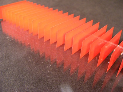
Lamination Technologies
Advanced Microfabrication
Project Overview
Microfabricated Laminations
In order to create a multilayer structure with sub-micron characteristic lengths, alternating layers of two or more metals are sequentially electroplated through a standard photoresist mold defined using photolithography techniques. The figure shows a conceptual rendering of the robotically-assisted electroplating setup. By automatically alternating the plating materials and controlling the electrodeposition time and current density, it is possible to create a thick (several hundreds of microns) structure that consists of sub-micron-thick layers of metallic materials. Post-electrodeposition, one or more metals are selectively etched away, creating a scaffold consisting of high-lateral-aspect-ratio metallic films. The metallic layers can be supported by metallic or polymer posts depending on the targeted application. For example, in highly-laminated magnetic cores, the layers must be electrically insulated from each other to efficiently reduce eddy current losses, preventing the use of metallic posts. Conceptually, this approach solely relies on established large area microfabrication techniques such as electroplating and chemical etching to develop a nanostructured material with improved performance.

Publications
- J. Kim, M. Kim, P. Galle, F. Herrault, R. Shafer, J.Y. Park, and M.G. Allen, “Nanolaminated permalloy core for high-flux high-frequency ultracompact power conversion,” Transactions on Power Electronics,v 28, n 9, p 4376-4383, Sept. 2013. (PDF)
- M. Kim, F. Herrault, J. Kim, J.K. Kim, and M.G. Allen, “Monolithically-fabricated laminated inductors with electrodeposited silver windings,” IEEE International Conference on Micro Electro Mechanical Systems (MEMS), p 873-876, Jan. 2013. (PDF)
- A. Armutlulu, Y. Fang, S.H. Kim, C.H. Ji, S.A. Bidstrup Allen, and M.G. Allen, ” A MEMS-enabled 3D zinc-air microbattery with improved discharge characteristics based on a multilayer metallic substructure,” Journal of Micromechanics and Microengineering, v 21, n 10, Oct. 2011. (PDF)
- F. Herrault, W.P. Galle, R.H. Shafer, and M.G. Allen, “Electroplating-based approaches for volumetric nanomanufacturing,” Technologies for Future Micro-Nano Manufacturing, Aug. 2011. (PDF)
- W.P. Galle, S.-H. Kim, U. Shah, and M.G. Allen, “Micromachined capacitors based on sequential multilayer electroplating,” 23nd IEEE International Conference on Micro Electro Mechanical Systems (MEMS 2010), Jan. 2010. (PDF)
- A. Armutlulu, Y. Fang, S.-H. Kim, C.-H. Ji, S.A. B. Allen, and M.G. Allen, “High-current Zn-Air microbattery based on a micromachined multilayer lateral metallic scaffold,” 10th International Workshop on Micro and Nanotechnology for Power Generation and Energy Conversion Applications (PowerMEMS 2010), p 107-110, 2010. (PDF)
Metal Transfer Micromolding
Advanced Microfabrication
Project Overview
MTM Process
Publications
- S. Rajaraman, S.-O. Choi, M.A. McClain, J.D. Ross, M.C. LaPlaca, and M.G. Allen, “Metal-transfer-micromolded three-dimensional microelectrode arrays for in-vitro brain-slice recordings,” Journal of Microelectromechanical Systems, v 20, n 2, p 396-409, April 2011. (PDF)
- Y. Zhao, Y.K. Yoon, S.O. Choi, X. Wu, Z. Liu, and M.G. Allen, “Three dimensional metal pattern transfer for replica molded microstructures,” Applied Physics Letters, vol. 94, no. 2, 023301, 2009. (PDF)
- S. Rajaraman, Y. Zhao, X. Wu, S.-H. Kim, and M.G. Allen, “Metal transfer micromolding (MTM) process for high-aspect-ratio 3-D structures with functional metal surfaces,” International Symposium on Flexible Automation (ISFA 2008), Atlanta, USA, June 2008. (PDF)
- S. Rajaraman, M.A. McClain, S.-O Choi, J.D. Ross, S.P. DeWeerth, M.C. LaPlaca, and M.G. Allen, “Three-dimensional metal transfer micromolded microelectrode arrays (MEAS) for in-vitro brain slice recordings,” Transducers 2007: The 14th International Conference on Solid-State Sensors, Actuators and Microsystems, pp.1251-1254, Lyon, France, June 2007. (PDF)
- Y. Zhao, Y.-K. Yoon, X. Wu, and M.G. Allen, “Metal-transfer-micromolding of air-lifted RF components,” Transducers 2007: The 14th International Conference on Solid-State Sensors, Actuators and Microsystems, Lyon, France, June 2007. (PDF)
- Y. Zhao, Y.-K. Yoon, and M.G. Allen, “Metal-transfer-micromolded RF components for System-On-Package (SOP),” 57 Electronic Components and Technology Conference (ECTC ’07), 2007. (PDF)
- S-O. Choi, S. Rajaraman, Y-K. Yoon, X. Wu, and M.G. Allen, “3-D metal patterned microstructure using inclined UV exposure and metal transfer micromolding technology,” Solid-State Sensor, Actuator, and Microsystems Workshop (Hilton Head 2006), June 2006. (PDF)
- X. Wu, Y. Zhao, Y.-K. Yoon, S.-O Choi, J.-H. Park and M.G. Allen, “Enhanced wettability polymer micromolding by a 3-D metal transfer process,” ACS conference, March 2006. (PDF)
UV-LED Lithography
Microfabrication technologies
Project Overview
UV-LED Performance Evaluation

Publications
- J.K. Kim, S.J. Paik, F. Herrault, and M.G. Allen, “UV-LED lithography for 3-D high aspect ratio microstructure patterning,” 14th Solid State Sensors, Actuators, and Microsystems Workshop, p 481-484, June 2012. (PDF)
- J.K. Kim, M.G. Allen, and Y.-K. Yoon, “Computer controlled dynamic mode multidirectional UV lithography for 3-D microfabrication,” Journal of Micromechanics and Microengineering, v 21, n 3, p 035003, March 2011. (PDF)
Biodegradable Sensors
Biomedical Implants
Project Overview
Biodegradable Pressure Sensors

Publications
- M. Luo, C. Song, F. Herrault, and M.G. Allen, “A microfabricated RF wireless pressure sensor made completely of biodegradable materials,” 14th Solid State Sensors, Actuators, and Microsystems Workshop, p 38-41, June 2012. (PDF)
MEMS-based batteries
Energy Storage
Project Overview
Microfabricated High-Surface-Area Batteries
Publications
- A. Armutlulu, S.A. Bidstrup Allen, and M.G. Allen, “3D microstructures for fast charge and discharge batteries,” PowerMEMS 2012, p 203-206, Dec. 2012. (PDF)
- J.K. Kim, A. Armutlulu, M. Kim, S. Paik, S.A. Bidstrup Allen, and M.G. Allen “A fabric-based Ni-Zn battery using a microfiber substrate and separator,” PowerMEMS 2012, p , Dec. 2012. (PDF)
- A. Armutlulu, Y. Fang, S.H. Kim, C.H. Ji, S.A. Bidstrup Allen, and M.G. Allen, ” A MEMS-enabled 3D zinc-air microbattery with improved discharge characteristics based on a multilayer metallic substructure,” Journal of Micromechanics and Microengineering, v 21, n 10, Oct. 2011. (PDF)
- A. Armutlulu, Y. Fang, S.-H. Kim, C.-H. Ji, S.A. B. Allen, and M.G. Allen, “High-current Zn-Air microbattery based on a micromachined multilayer lateral metallic scaffold,” 10th International Workshop on Micro and Nanotechnology for Power Generation and Energy Conversion Applications (PowerMEMS 2010), p 107-110, 2010. (PDF)
Air-Flow Sensors
Flight Control Applications
Project Overview
Piezoresistive Air-Flow Sensors
formed from laser-machined polyimide and PECVD-deposited silicon dioxide, and a conductive elastomer piezoresistor with a measured gage factor of 7.3 located at the base of the microtuft. The fabrication sequence also enables backside interconnects without adding further process complexity, which facilitates integration and enables the sensing of airflow with minimum interference due to the sensing circuitry. Individual microtufts as small as 1.5 mm in length and 0.4 mm in width, with 70-micron-wide piezoresistor lines have been fabricated, and operation has been demonstrated in wind tunnel.
Publications
- C. Song, A.R. Aiyar, S.-H. Kim, and M.G. Allen, “Exploitation of aeroelastic effects for drift reduction, in an all-polymer air flow sensor,” Sensors and Actuator: A Physical, v 165, n 1, p 66-72, Jan. 2011. (PDF)
- A.R. Aiyar, C. Song, S.-H. Kim and M. G. Allen, “An all-polymer air-flow sensor array using a piezoresistive composite elastomer,” Smart Materials and Structures, 18, 115002, 2009. (PDF)
- C. Song, A. R. Aiyar, S.-H. Kim, and M.G. Allen, “Exploitation of aeroelastic effects for drift reduction in an all-polymer air flow sensor,” Solid-State Sensors, Actuators and Microsystems Conference (TRANSDUCERS 2009), pp. 1545-1548, June 2009. (PDF)
- A. Aiyar, C. Song, S.-H. Kim, and M.G. Allen, “An all polymer air-flow sensor array using a piezoresistive composite elastomer,” 22nd IEEE International Conference on Micro Electro Mechanical Systems (MEMS 2009), pp. 447-451, Jan. 2009. (PDF)
Microneedle Patch
Project Overview
Microneedle Patch
We are working towards developing a technology for the painless, self-monitoring of blood glucose concentrations using a patch-type smart microneedle module. The system consists of a patch-type smart microneedle module with integration of minimally-invasive microneedles and micro/nano porous sensing microelectrodes; and a handheld monitor module that remotely receives sensing results and analyzes the data. A 3-D microstructure with sharp tip end and high aspect ratio penetrates skin in a minimally invasive manner, and micro/nano porous sensing microelectrodes detect glucose molecules in the body. The 3-D microneedle structure and isolated microelectrodes are fabricated at Georgia Tech and are integrated with micro/nano porous electrodes developed in collaboration with Kwangwoon University.
Collaboration: Kwangwoon University, South Korea, and Infopia, South Korea
Sponsor: Korea Institute for Advancement of Technology (KIAT)

Publications
Small-Scale Reed Actuators
Heat Transfer Enhancement Technology
Project Overview
Flow-Powered Passive Reed Actuators
Collaboration: Pr. A. Glezer’s research group at Goergia Tech (Fluid Mechanics Research Group)
Sponsor: DARPA
Publications
- F. Herrault, P.A. Hidalgo, C.-H. Ji, A. Glezer, and M.G. Allen, “Cooling performance of micromachined self-oscillating reed actuators in heat transfer channels with integrated diagnostics,” IEEE International Conference on Micro Electro Mechanical Systems (MEMS), p 1217-1220, Jan. 2012. (PDF)
- P. Hidalgo, F. Herrault, A. Glezer, M.G. Allen, S. Kaslusky, and B. S.Rock, “Heat transfer enhancement in high-power heat sinks using active reed technology,” 16th International Workshop on Thermal Investigations of ICs and Systems (THERMINIC), Page(s): 1-6, v 19, Oct. 2010. (PDF)
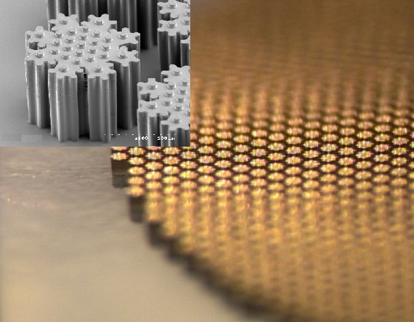
Silicon Nanoneedles
Intracellular Drug Delivery
Project Overview
Micromachined Silicon Nanoneedles
We are working, in collaboration with researchers of Dr. M.R. Prausnitz’s research group at Georgia Tech, towards developing highly-dense needle arrays with sharp nano-tips for intracellular gene and drug delivery, with the ultimate goal of gene correction in a high-throughput manner. The nanoneedles are fabricated using silicon micromachining technology including isotropic dry etching, anisotropic dry etching and thermal-oxidation-based tip sharpening. The silicon nanoneedle array with needle tip diameters in tens of nanometers enables pinpoint injection of individual cells in a high throughput manner without causing cell death by puncture. The image shows a dense array of such silicon needles with nano-tips. In-vitro intracellular delivery tests demonstrate that the nanoneedle array can effectively deliver molecular probes into cells by cell membrane penetration.
Collaboration: Laboratory for Drug Delivery – Pr. M. Prausnitz – Georgia Tech
Sponsor: National Institute of Health (NIH)

Publications
- S.J. Paik, S. Park, V. Zamitsyn, S. Choi, X. Guo, M. Prausnitz, and M.G. Allen, “A highly dense nanoneedle array for intracellular gene delivery,” 14th Solid State Sensors, Actuators, and Microsystems Workshop, p 149-152, June 2012. (PDF)
Elastomeric Microelectrodes
Neural Recordings
Project Overview
Highly-Compliant Microcable Neuroelectrodes
We develop a fabrication process flow for arrays of electrically functional, elastomer microcables. Elastomeric electronics is generally comprised of an elastomer that integrates an electrical conductor in some fashion, commonly by mixing conductive particulates into the bulk elastomer. Using bulk electrically conductive elastomers in micropatterned devices presents challenges in controlled, precise patterning of the conductive media and in incorporating the conductive component with selectively insulated and exposed regions. Thin-film gold metallization of silicone rubber addresses these considerations as gold is frequently patterned in microfabricated devices and silicone can tolerate some but not all standard process techniques. Gold has relatively soft and non-brittle mechanical properties, which are advantageous for use in elastomer electronics. It also does not form a surface oxide, making it suitable for features such as the electrical access nodes for this application. PDMS shape and topography is being defined using a spun-cast micromolding technology.
Publications
- M.A. McClain, I.P. Clements, R.H. Shafer, R.V. Bellamkonda, M.C. Laplaca, and M.G. Allen, “Highly-compliant, microcable neuroelectrodes fabricated from thin-film gold and PDMS,” Biomedical Microdevices, v 13, n 2, p 361-373, April 2011. (PDF)
- M.A. McClain, M.C. LaPlaca, and M.G. Allen, “Spun-cast micromolding for etchless micropatterning of electrically functional PDMS structures,” Journal of Micromechanics and Microengineering, v 19, n 10, p 107002 (6 pp.), Oct. 2009. (PDF)
- M. McClain, M. C LaPlaca, and M.G. Allen, “An integrated elastomer mesh and microelectrode array for neurophysiology,” Georgia Life Sciences Summit, September 2008.
- M.A. McClain, M.C. LaPlaca, and M.G. Allen, “The development of strand-like microelectrode arrays for in vitro neuron culture,” Society for Neuroscience, Nov. 2007.
Air-Core Inductors
Power Supply on a Chip
Project Overview
Microfabricated Air-Core Inductors
Collaboration: MIT
Sponsor: ARPA-e

Publications
- X. Yu, M. Kim, F. Herrault, C.-H. Ji, J. Kim, and M.G. Allen, “Silicon-embedding approaches to 3-D toroidal inductor fabrication,” Journal of Microelectromechanical Systems, in press.
- M. Araghchini, J. Chen, V. Doan-Nguyen, D.V. Harburg, D. Jin, J. Kim, M. Kim, S. Lim, B. Lu, D. Piedra, J. Qiu, J. Ranson, M. Sun, X. Yu, H. Yun, M.G. Allen, J.A. del Alamo, G. DesGroseilliers, F. Herrault, J.H. Lang, C.G. Levey, C.B. Murray, D. Otten, T. Palacios, D.J. Perreault, and C.R. Sullivan, “A technology overview of the powerchip development program,” Transactions on Power Electronics,v 28, n 9, p 4182-4201, Sept. 2013. (PDF)
- J.K. Kim, F. Herrault, X. Yu, M. Kim, R.H. Shafer, and M.G. Allen, “Microfabrication of air core inductors with metal-encapsulated polymer vias,” Journal of Micromechanics and Microengineering, v 23, n 3, p 035006 (7 pp.), March 2013. (PDF)
- J.K. Kim, F. Herrault, X. Yu, and M.G. Allen, “Microfabrication of air-core toroidal inductor with very high aspect ratio metal-encapsulated polymer vias,” PowerMEMS 2012, p 30-33, Dec. 2012. (PDF)
- X. Yu, M. Araghchini, F. Herrault, J.K. Kim. J.H. Lang, and M.G. Allen, “Fabrication, modeling and performance analysis of silicon-embedded 3-D toroidal inductors,” PowerMEMS 2012, p 58-61, Dec. 2012. (PDF)
- M. Araghchini, M. Kim, X. Yu, F. Herrault, M.G. Allen, and J.H. Lang, “Modeling and measured verification of loss in MEMS toroidal inductors,” IEEE Energy Conversion Congress and Exposition (ECCE), p 3293-3300, Sept. 2012. (PDF)
- D.V. Harburg, X. Yu, F. Herrault, C.G. Levey, M.G. Allen, and C.R. Sullivan, “Micro-fabricated thin-film inductors for on-chip power conversion,” 2012 7th International Conference on Integrated Power Electronics Systems (CIPS), p. 6ff, March 2012. (PDF)
- X. Yu, M.S. Kim, F. Herrault, C.-H. Ji, J.K. Kim, and M.G. Allen, “Silicon-embedded 3D toroidal air-core inductor with through-wafer interconnect for on-chip integration,” IEEE International Conference on Micro Electro Mechanical Systems (MEMS), p 325-328, Jan. 2012. (PDF)
- Y.-K. Yoon, J.-W. Park, and M.G. Allen, “Polymer-core conductor approaches for RF MEMS” Journal of Microelectromechanical Systems, v. 14, n. 5, Oct, 2005. (PDF)
Laminated Metallic Magnetic Cores
Power Supply on a Chip
Project Overview
Laminated Metallic Magnetic Cores
Sponsor: ARPA-e

Publications
- J. Kim, M. Kim, P. Galle, F. Herrault, R. Shafer, J.Y. Park, and M.G. Allen, “Nanolaminated permalloy core for high-flux high-frequency ultracompact power conversion,” Transactions on Power Electronics,v 28, n 9, p 4376-4383, Sept. 2013. (PDF)
- M. Kim, F. Herrault, J. Kim, J.K. Kim, and M.G. Allen, “Monolithically-fabricated laminated inductors with electrodeposited silver windings,” IEEE International Conference on Micro Electro Mechanical Systems (MEMS), p 873-876, Jan. 2013. (PDF)
- J. Kim, J.K. Kim, M. Kim, F. Herrault, and M.G. Allen, “Integrated toroidal inductors with nanolaminated metallic magnetic cores,” PowerMEMS 2012, p 18-21, Dec. 2012. (PDF)
- F. Herrault, W.P. Galle, R.H. Shafer, and M.G. Allen, “Electroplating-based approaches for volumetric nanomanufacturing,” Technologies for Future Micro-Nano Manufacturing, Aug. 2011. (PDF)
- W.P. Galle, S.-H. Kim, U. Shah, and M.G. Allen, “Micromachined capacitors based on sequential multilayer electroplating,” 23nd IEEE International Conference on Micro Electro Mechanical Systems (MEMS 2010), Jan. 2010. (PDF)
- P. Galle, X. Wu, L. Milner, S.-H. Kim, P. Johnson, P. Smeys, P. Hopper, K. Hwang, and M.G. Allen, “Ultra-compact power conversion based on a CMOS-compatible microfabricated power inductor with minimized core losses,” 57 Electronic Components and Technology Conference (ECTC ’07), 2007. (PDF)
- J.-W. Park, F. Cros, and M.G. Allen, “Planar spiral inductors with multilayer micrometer-scale laminated cores for compact-packaging power converter applications,” IEEE Transactions on Magnetics, v 40, no. 4, July 2004. (PDF)
- J.-W. Park, and M.G. Allen, “Ultra low-profile micromachined power Inductors with highly laminated Ni/Fe cores: Application to low-megahertz DC-DC converters,” IEEE Transactions on Magnectics, vol. 39, no. 5, pp. 3184-3186, Sept. 2003. (PDF)
- J.W. Park, J. Park, Y.-H. Joung, and M.G. Allen, “Fabrication of high current and low profile micromachined inductor with laminated Ni/Fe core,” IEEE Transactions on Components and Packaging Technologies, vol. 25, no. 1, p. 106-111, 2002. (PDF)
- J.-W. Park, F. Cros, and M.G. Allen, “A sacrificial layer approach to highly laminated magnetic cores,” 15th IEEE International Conference on Micro Electro Mechanical Systems (MEMS), p.380-3, 2002. (PDF)
Microfabricated Permanent-Magnet Arrays
Small-Scale Undulators for X-Ray Generation
Project Overview
Laser-Micromachined Permanent Magnets
Many MEMS systems can benefit from dense, alternating arrays of permanent magnets (PM) with high energy-product and substantial magnetic flux density adjacent to the array. In this work, we demonstrate laser machining fabrication and assembly techniques to create linear PM alternating arrays with periods as low as 230 microns. Comb-shaped magnet structures are micromachined from a 300 micron thick samarium cobalt (SmCo) substrate using an IR laser. These structures are then magnetized and assembled in an interlocking fashion to make alternating magnet arrays of various total lengths. Scanning Hall-effect sensor measurements taken 80 microns above the surface indicate sinusoidally varying magnetic fields with periods as expected from the underlying magnet geometry and peak magnetic flux density amplitudes of 0.1 T.
Collaboration: Pr. D. Arnold’s research group at the University of Florida
Sponsor: DARPA

Publications
- B.A. Peterson, W.C. Patterson, F. Herrault, D.P. Arnold, and M.G. Allen, “Laser-micromachined permanent magnet arrays with spatially alternating magnetic field distribution,” PowerMEMS 2012, p 319-322, Dec. 2012. (PDF)
- B.A. Peterson, F. Herrault, O.D. Oniku, Z.A. Kaufman, D.P. Arnold, and M.G. Allen, “Assessment of laser-induced damage in laser-micromachined rare-earth permanent magnets at the sub-millimeter scale,” IEEE Transactions on Magnetics, v 48, n 11, p 3606-9, Nov. 2012. (PDF)
- B.A. Peterson, F. Herrault, O.D. Oniku, Z.A. Kaufman, D.P. Arnold, and M.G. Allen, “Assessment of laser-induced damage in laser-micromachined rare-earth permanent magnets at the sub-millimeter scale,” Intermag 2012, May 2012.
Polymer Microneedles
Transdermal Drug Delivery
Project Overview
Polymer Microneedles
We are working towards developing low-cost batch-fabricated single-use microneedle arrays for transdermal drug delivery. Drug delivery through micro-fabricated needles is of great interest for its capability to transport pharmaceutical and therapeutic agents, virus-like-particles, and other molecules into the body through the skin with minimal invasion and pain. Potential applications include regular immunizations (e.g., hepatitis B and measles) and annual inoculation (e.g., influenza). In this project, different types of microneedles have been successfully designed, fabricated (as shown in these images), and characterized for fluidic functionality and skin penetrability. Package, drug delivery, as well as safety are also under investigation with researchers at Georgia Tech and Emory University to reach clinical use of microfabricated needles.
Collaboration: Pr. M. Prausnitz’s research group at Georgia Tech
Sponsor: NIH
- J. Kim, S.-J. Paik, P.-C. Wang, S.-H. Kim, and M.G. Allen, “Maskless fabrication of high aspect ratio structures by combination of micromolding and direct drawing,” 24th IEEE International Conference on Micro Electro Mechanical Systems (MEMS2011), pp.280-283, Cancun, Mexico, Jan. 2011. (PDF)
- P.-C. Wang, S.-J. Paik, J. Kim, S.-H. Kim, and M.G. Allen, “Hypodermic-needle-like hollow polymer microneedle array using UV lithography into micromolds,” 24th IEEE International Conference on Micro Electro Mechanical Systems (MEMS2011), v 165, n 1, p 66-72, Jan. 2011. (PDF)
- S.-J. Paik, S.-H. Kim, P.-C. Wang, B. Wester, and M.G. Allen, “Dissolvable-tipped, drug-reservoir integrated microneedle array for transdermal drug delivery,” 23rd IEEE International Conference on Micro Electro Mechanical Systems (MEMS 2010), pp. 312 – 315, Jan. 2010. (PDF)
- P.-C. Wang, B. A. Wester, S. Rajaraman, S.-J. Paik, S.-H. Kim, and M.G. Allen, “Hollow polymer microneedle array fabricated by photolithography process combined with micromolding technique,” IEEE EMBC conference, Sept. 2009. (PDF)
- J.-H. Park, Y.-K. Yoon, S.-O Choi, M.R. Prausnitz, and M.G. Allen, “Tapered conical polymer microneedles fabricated using an integrated lens technique for transdermal drug delivery,” IEEE Transactions on Biomedical Engineering, v 54, n 5, p 903-13, May 2007. (PDF)
- J.-H. Park, M.G. Allen, and M.R. Prausnitz, “Biodegradable polymer microneedles: fabrication, mechanics and transdermal drug delivery,” Journal of Controlled Release, 104:51-66, 2005. (PDF)
- Microtweezers
- Tactile Displays
- Piezoelectric Actuators
- MicroElectrode Arrays
- Implantable Pressure Sensors
- Microneedles
- Solar Cells
- Electrets
- Force sensors
- Micro Pulsejets
- Conductive-Fuel Actuators
- Gas Generators
- Micro Power Converters
- Magnetic Generators
- MEMS Resonant Compass
- Acoustic Sensors
- Magnetic Relays
- Inclined Nanoimprinting
- Nanojets
- MEMS for Nanopatterning
- Ferroelectric RF Capacitors
- RF Inductors
- mm-Wave Antennas
- HT Chemical Sensors
- Capacitive Pressure Sensors
- RF Flow Sensors